Location:Home > Attention
PCB design considerations
First, pads and holes
1. Overlap placement of holes will cause broken drill bits and wire damage due to multiple holes during drilling. The distance between the holes should be ensured above 16mil (0.4mm) or the holes will be broken.
2. The length / width ratio of the special-shaped hole should be ≥ 1: 2.3, and the width should be> 0.8mm. If the two ends of the slot hole require a right angle, it is necessary to open the mold; if the two ends of the slot are oval, CNC drilling can be used.
3. Hole size. Some components are round and some are square. Please design the hole diameter to be 0.2mm or more than the diameter or square diagonal dimension for easy insertion.
4. If there are holes that do not require metallization (NPTH) on the double panel, it should be stated separately.
5. If there are grooves to be milled in the PCB, please use Keep Out Layer to draw them. Do not use pad filling to avoid mismilling or missing milling.
6. The thickness of the double-panel of the pad corresponding to the aperture of the conventional design is 24mil (0.6mm) larger than the aperture, the outer diameter of the via is 16mil (0.4mm) larger than the hole, and the single-panel is 31mil (0.8mm) larger than the aperture. .
Second, the line
1. The grid line spacing line and line are below 8mil, which will cause the connection to become a large copper surface line during the printing process.
2. The copper surface of the line should be 16mil (0.4mm) from the edge of the board to meet the UL regulations, so that copper will not be damaged during the gong board.
3. Outer layer design line width / spacing: 1oz 7mil / 7mil (0.1778mm / 0.1778mm) on one side
Single-sided 2oz sheet 8mil / 8mil (0.203mm / 0.203mm)
Double-sided 1 / 2oz sheet 5mil / 5mil (0.127mm / 0.127mm)
Double-sided 2oz sheet 8mil / 8mil (0.203mm / 0.203mm)
Double-sided 3oz sheet 10mil / 10mil (0.253mm / 0.253mm)
4. Place the line between the two PADs. Do not draw intermittently, it is best to connect one to the end. If a thick line is required, you can directly place a thick line. Do not repeat the thin line to achieve a thicker effect. It is easy to modify when modifying the line.
Third, solder mask
When designing with Protel, a large area of tin or a TOP layer of solder wire should be Top Solder Mask, and the Bottom layer should be Bottom Solder Mask.
Characters
1. Characters cover PAD, continuity test and component welding bring inconvenience and affect welding reliability.
2. The character design is too small, making screen printing difficult and making the characters unclear. Character height ≥25MIL, width ≥5MIL
Five, test
1. Flying probe test The test speed is slow. It is generally used to test samples.
2. Template testing. One is a simple test mold with a surface IC pad width greater than 0.6MM. This test template can be disassembled and the test pin can be reused at a relatively low cost. The other is a product with a large number of ICs on the test surface of the composite mold and a large number of points. This kind of production is complicated and impossible to disassemble and the cost is high.
Forming
1. pcb board less than 50mm * 50mm needs to be designed in the form of V-cut or die-cutting.
2. If the V-cut processing method is adopted, the distance between the two lines between the panels is half of the plate thickness, that is, the distance between the V-cut line and the forming line is 1/4 of the plate.
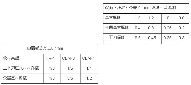
3. The thickness of V-cut residual thickness is not specified in the following table:
4, long board, small board, V cutting residual thickness residual negative difference. If there are special requirements for the residual thickness of a certain type of plate, you can specify the residual thickness data or our company can provide several types of residual thickness samples to choose. In addition, for long and narrow boards, micro boards, or components with special side boards, a splitter is recommended.