
Location:Home > Attention
1. Verify that the greatest continuous unpierced area of conductor does not exceed the maximum area diameter specified in Table I of the descriptive pages in this
Detect the largest continuous unperforated conductor area that does not exceed the maximum diameter area specified in Table I on the description page of this step
COMPONENT-PRINTED WIRING BOARDS (ZPMV2, ZPMV3)
Procedure.This may be accomplished by determining the largest circle which can be inscribed on the unpierced conductor portion of the printed wiring board (see Figure 1.)
Step: This can be done by defining the maximum circle that can be inscribed in the conductor area of the unperforated printed circuit board (Figure: Figure 1)
Figure 1
MAXIMUM UNPIERCED AREA
DIAMETER MEASUREMENT
Maximum unperforated area diameter measurement
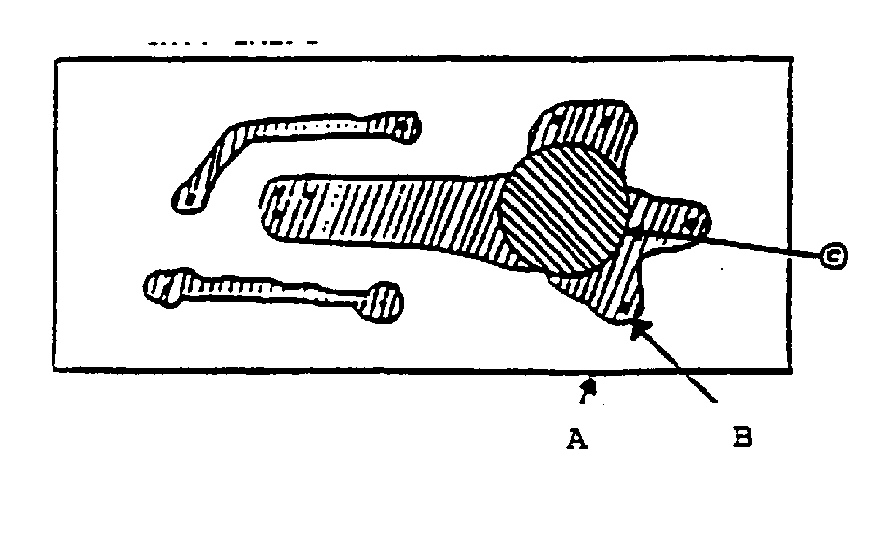
A-Production printed wiring board.
Production of printed circuit boards
B-Largest unpierced conductor section.
Maximum unperforated conductor area
C-Largest circle that can be inscribed on B.
Maximum circle that can be inscribed in B (25.4mm)
If it is larger than 25.4mm, a small circle can be cut in the middle of the copper surface to solve this related requirement.
The thinnest line width in the board design is 0.11MM The thinnest line width nearest to the board edge is 0.17MM
MIDBOARD CONDUCTOR-A conductor spaced more than 1/64 in. (0.4 mm) from the edge of a printed wiring board.
Conductor in board-Conductor is more than 1/64 inch (0.4mm) from edge of printed circuit board
As shown
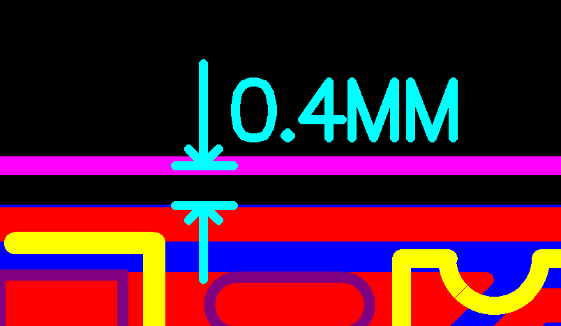
Because the tolerance of the machine tool plus or minus 0.2MM is recommended to be greater than 0.6MM to ensure that each PCSW meets UL regulations.
Detect the largest continuous unperforated conductor area that does not exceed the maximum diameter area specified in Table I on the description page of this step
COMPONENT-PRINTED WIRING BOARDS (ZPMV2, ZPMV3)
Procedure.This may be accomplished by determining the largest circle which can be inscribed on the unpierced conductor portion of the printed wiring board (see Figure 1.)
Step: This can be done by defining the maximum circle that can be inscribed in the conductor area of the unperforated printed circuit board (Figure: Figure 1)
Figure 1
MAXIMUM UNPIERCED AREA
DIAMETER MEASUREMENT
Maximum unperforated area diameter measurement
A-Production printed wiring board.
Production of printed circuit boards
B-Largest unpierced conductor section.
Maximum unperforated conductor area
C-Largest circle that can be inscribed on B.
Maximum circle that can be inscribed in B (25.4mm)
If it is larger than 25.4mm, a small circle can be cut in the middle of the copper surface to solve this related requirement.
The thinnest line width in the board design is 0.11MM The thinnest line width nearest to the board edge is 0.17MM
MIDBOARD CONDUCTOR-A conductor spaced more than 1/64 in. (0.4 mm) from the edge of a printed wiring board.
Conductor in board-Conductor is more than 1/64 inch (0.4mm) from edge of printed circuit board
As shown
Because the tolerance of the machine tool plus or minus 0.2MM is recommended to be greater than 0.6MM to ensure that each PCSW meets UL regulations.